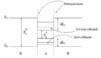
Fig. (i) Type I superlattice GaAs/AlAs

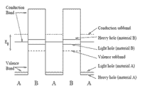
Fig. (ii) Type II superlattice InAs/InGaSb

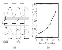
Fig. (iii) Energy bands (a) and cut-off wavelength in InAs/GaSb SLs vs. InAs layer thickness
Infrared sources and detectors have found widespread scientific and industrial applications in mid-to-long infrared (IR) imaging systems.The principle applications of such materials in the past have been for military only - to detect and track hot objects at long range, to provide completely passive night-vision and to give assisted daytime vision when the atmospheric transmission in the visible is poor due to smoke or dust. This technology of thermal imaging and night-vision, based on IR radiation in the 8-14 micron atmospheric window not affected by water vapor is now becoming increasingly exploited outside the military arena : for example in see-through-smoke applications associated with fire fighting, thermal imaging of people buried in collapsed buildings, surveillance, security and bio-medical imaging etc. It is quite likely that the future requirements of energy efficiency in housing and other structures and processes will make IR imaging a routine technique for discovering the potential energy leaks. Monitoring the properties of the earth both with respect to temperature (global warming) and chemically will certainly require advanced IR detectors that are suitably reliable for applications in satellites for surveillance of the earth from the space.
All of these applications bode well for the unique niche that the novel IR semiconductor materials fill. The earlier military applications withstood the expense of less stable and convenient material such as HgxCd1-xTe mercury-cadmium telluride (MCT) alloy. However, there have been difficulties associated with fabricating high performance MCT arrays, especially for 10 micrometers. The major difficulties are: (i) compositional inaccuracies cause variations of the band gap , (ii) large tunneling dark currents caused by the narrow band gap (< 0.1 eV) and the small effective mass result in low specific detectivities, and (iii) high Auger recombination rates further increase the dark current. The emergence of thin film growth techniques such as molecular beam epitaxy (MBE) and metal organic chemical vapor deposition (MOCVD) has allowed the synthesization of a wide range of multiple quantum wells (MQWs) and SL material systems. Such artificial structures are currently of great interest as they afford the possibility of tailoring the electronic structure by controlled modification of the growth parameters: viz., layer thickness, alloy composition, strain, growth orientation, etc.
Recently, the interest in lattice matched multi-quantum wells and SLs has brought the promise of faster electronics, via high electron mobility transistors, and improved lasers. The growth of novel thin strained layer SLs on established substrates has opened up new methods of IR detection applications. Now, the prospects of replacing MCT alloy with strained layer III-V SLs is very promising, and the pace of development has been particularly rapid in recent years. The strained layer InAs/InxGa1-xSb SLs are suggested to have electronic and optical properties superior to those of MCT. Detectors based on such SLs can be readily manufactured owing to its compatibility with advanced III-V device processing technology and to the enhanced structural stability of the material. In type-II SLs, the long wavelengths are possible because of the strong misalignment of the band edges of the two host materials at the interface: the conduction band edge of InAs lies well below the valence band edge of InxGa1-xSb. For sufficiently thin InAs and/or InGaSb layers the sum of the quantization energies of electrons and holes exceeds the band overlap between the InAs conduction band and the InGaSb valence band. As a consequence, a spatially indirect SL band gap opens up between the topmost quantized hole state in the InGaSb layers and the lowest confined electron level in InAs layers. Thus, the SL band gap, which determines the infrared (IR) optical properties of InAs/InGaSb SLs can be tailored' through the entire mid- and far-IR spectral region by varying the individual layer thickness. This property makes InAs/InGaSb SLs interesting for applications in IR detectors as well as in IR lasers.
The motivation of the present comprehensive theoretical project is to examine the usefulness of type II InAs/InxGa1-xSb SL material systems for IR detectors. For device purposes, we will focus our attention on studying the effects of superlattice parameters (viz., the layer thickness of InxGa1-xSb and InAs; alloy composition x; strain; interfacial chemistry; and the growth orientation) on the SL energy band gaps, electron effective masses [both parallel (in-plane) and perpendicular (along the growth axis) to the SL], absorption coefficient and detectivity D*. The prime motivation of this study has been to map the available parameter space in search of material and layer combinations suitable for the IR detector applications.